
The research environment in Toyohashi University of Technology is very blessed. Because We have only one Electron Device Reserch Center in Japan that enable Designing, fabricating and evaluating 2-inch and 4-inch level device.
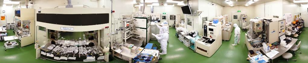
Electron Device Research Center
| Ultra-pure water plants | Clean bench for chemical treatment |
| N2 blower | Wafer spinning drier |
| Oxidation/Annealing furnace for 4 inch wafer | Phosphorus diffusion furnace for 4 inch wafer |
| Ion implantation equipment | Al Sputter |
| Metal (3 targets) Sputter | PL-CVD for Poly-Silicon |
| PL-CVD for TEOS-SiO2 & Si3N4 | PEDVD for BPSG |
| Reactive Ion Etching(RIE) of silicon | RIE for metal |
| O2 ashing equipment | Anisotropic wet etching system(TMAH) |
| EB lithography exposure | g line stepper |
| i line stepper | Resist coater/developer |
| Spinner | Spray coater |
| Projection aligner | Mask aligner |
| Contact aligner for 2 inch wafer | Contact aligner for 4 inch wafer |
| Gold wire bonding | Die bonder |
| Dicing equiment | Anodic bonding apparatus |
| Vacuum anodic bonding apparatus | Wafer probing system |
| Variable temperature probing system | Hg probing system |
| Semiconductor parameter analyzer | LCR impedance analyzer |
| Wafer flatness tester | Ellipsometer |
| Spectroscopic ellipsometer | Surface profiler |
| Laser microscope | FE-SEM |
| Optical microscope | 4 point probe |
| Cadence for mask design | SPICE for device simulation |
| SUPREM for process simulation | ANSYS for analysis system |
| SPECTRA for device simulation | TOCCATA for lighting simulation software |
Electron Device Research Center
Venture Business Laboratory
| ICP etching equipment | Reactive ion etching equipment |
| XeF2-Si etching equipment | Sputter equipment (3 targets) |
| Plasma CVD equipment | H2 gas annealing furnace for 4 inch wafer |
| Oxidation/Annealing furnace for 4 inch wafer | Annealing furnace for 2 inch wafer |
